Buried Pad PCB Fixing
Checkout how we drilled through the back of a PCB in order to solder to the hidden pads under a cellular module.

SOIC footprint with one edge of reversed pins
I've often said, "Anyone can make a PCB, but it takes real skill to make a bad PCB good." This is really just a way to excuse myself when I screw up a design.
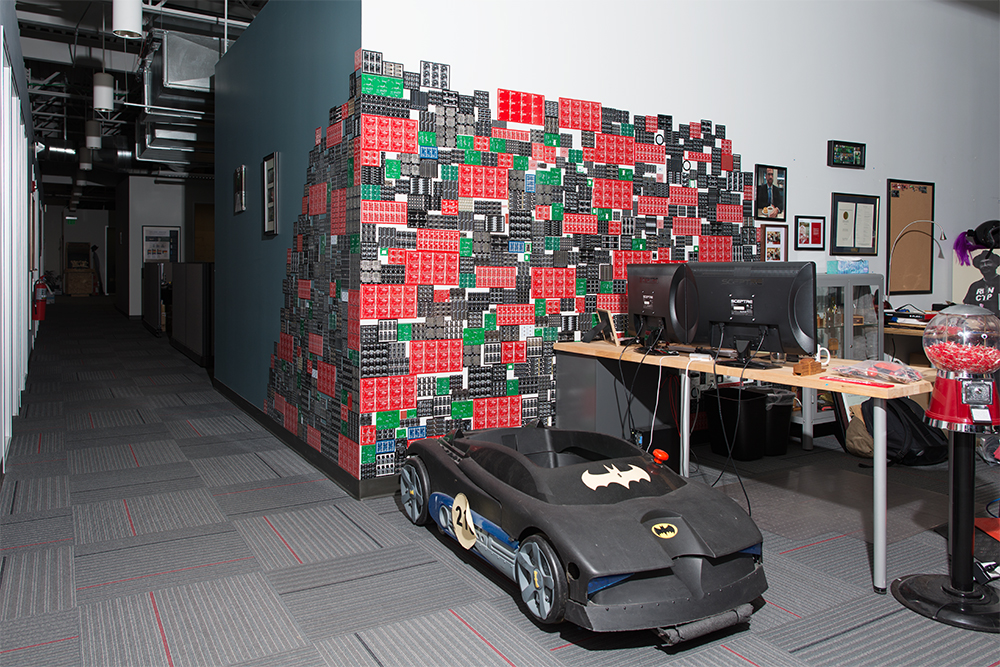
SparkX wall of Unabashed Failure
We have a wall in the SparkX area where we’ve nailed our bad PCBs around a corner. These are all the PCBs we’ve messed up over the last two years. We’ve been busy. Each one of theses designs (should) tell a different story. Many companies deny they ever make mistakes. Life is too short. We are unabashed with our failures. We nail them to the wall and tell everyone about them so we don’t make the same mistake again.
The wall of wonderful screw ups at SparkX
I've been designing boards (and fouling them up) for nearly two decades. I’ve learned many tricks but the biggest lesson is to make sure, regardless of the number of cut traces or green wire fixes need to be made, that 100 percent of the circuit is working before you order another round of boards. If you just find the first error and order new boards, you’ll quickly discover you just fixed the first error. However, on my latest project I had to do a maneuver that I haven't seen or tried before so I thought I’d share.

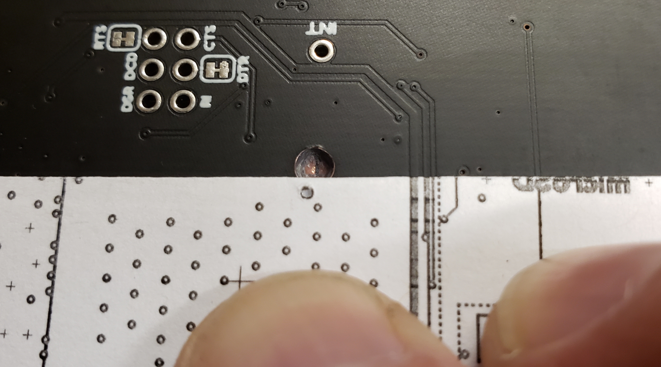
How do I get to that pad?
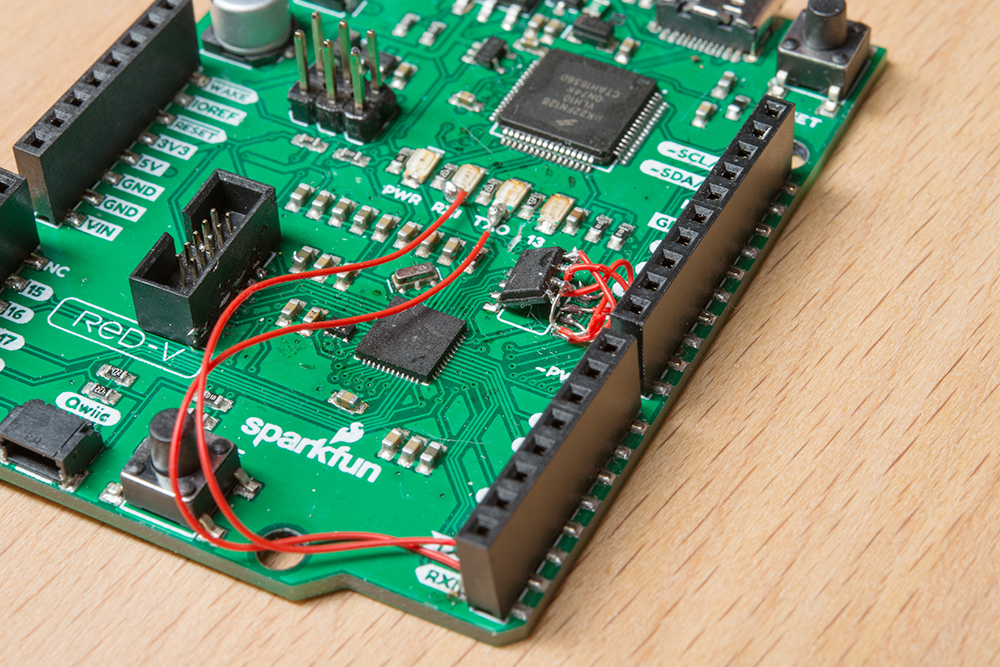
This particular prototype is a combination of Artemis and our LTE cellular module. Nothing too wild. As with most prototypes I started with a RedBoard Artemis and the LTE shield to make sure everything would work. I then laid out a board and had a few protos built. As I started bringing up the various parts of the board everything worked, except I couldn’t get the cellular to turn on...
SARA-PWR pad to nowhere
I can make all sorts of excuses (I had too many projects at the same time, was moving too fast, yadda, yadda), but I completely neglected to route the power pin from the SARA module to Artemis.
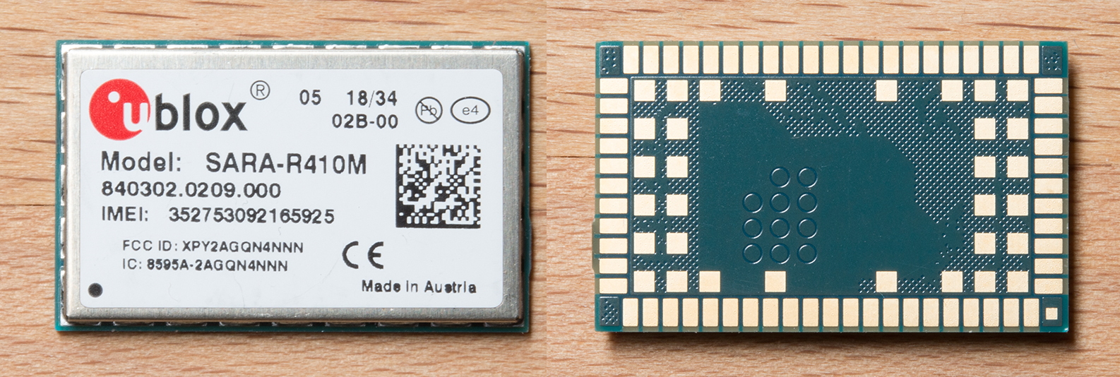
The front / rear of the Ublox SARA module
The SARA LTE NB-IoT cellular module has an incredible feature set and, like many cellular modules, has a power pin that has to be held low for two or three seconds for the module to start up. On a normal design, the IC legs are exposed. It’s easy to solder to a SOIC or TSSOP. With a little sticky tack (to hold the wire in place), flux, wire wrap wire and some solder wick, you can even solder to QFN devices. The SARA module is a little unique in that the pads are directly underneath the module. There is no copper or pad exposed from underneath the module. And similarly unique, the pads on the bottom of the module are quite large (as compared to a QFN). I had a choice: I could either have a new round of PCBs made, or I could try to drill through the bottom of the PCB, stop before I rip the pad on the bottom of the SARA module, and somehow get hot solder and a wire onto the power control pad. So let’s do that.
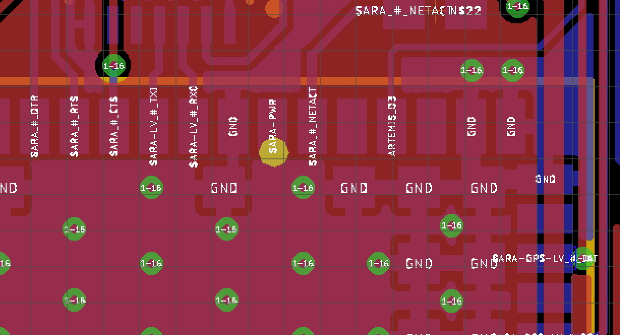
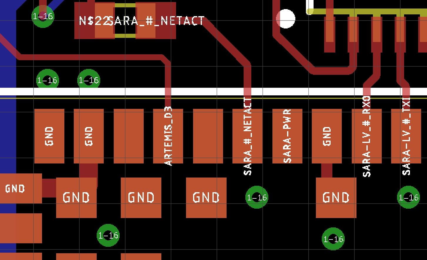
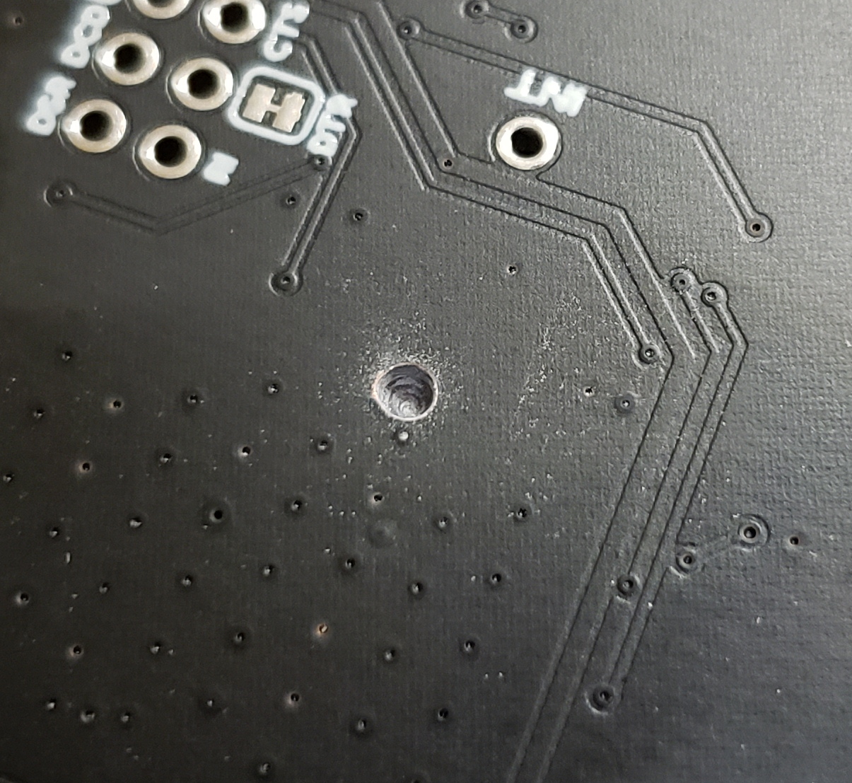
Location of the pad as seen from the rear of the board
Step one was locating the exact spot to drill on the back of the board. I opened the Eagle design, flipped it and added a 1/16-inch dot where I wanted to attach. I made the dot bridge the gap between the pad I needed and the ground pour near by. This was intentional - once the hole was in place, the straight line of the ground pad would help me navigate to the center location of the power control pad.

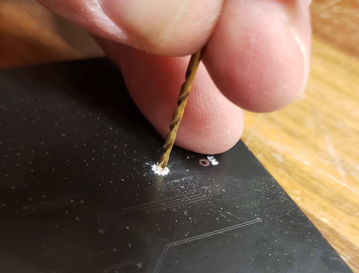
Spring loaded center punch marks the spot
I printed a 1:1 scale drawing. I cut out the rectangle and lined it up with the back of the proto. Using a center punch I made a small indentation where the hole needed to be made.
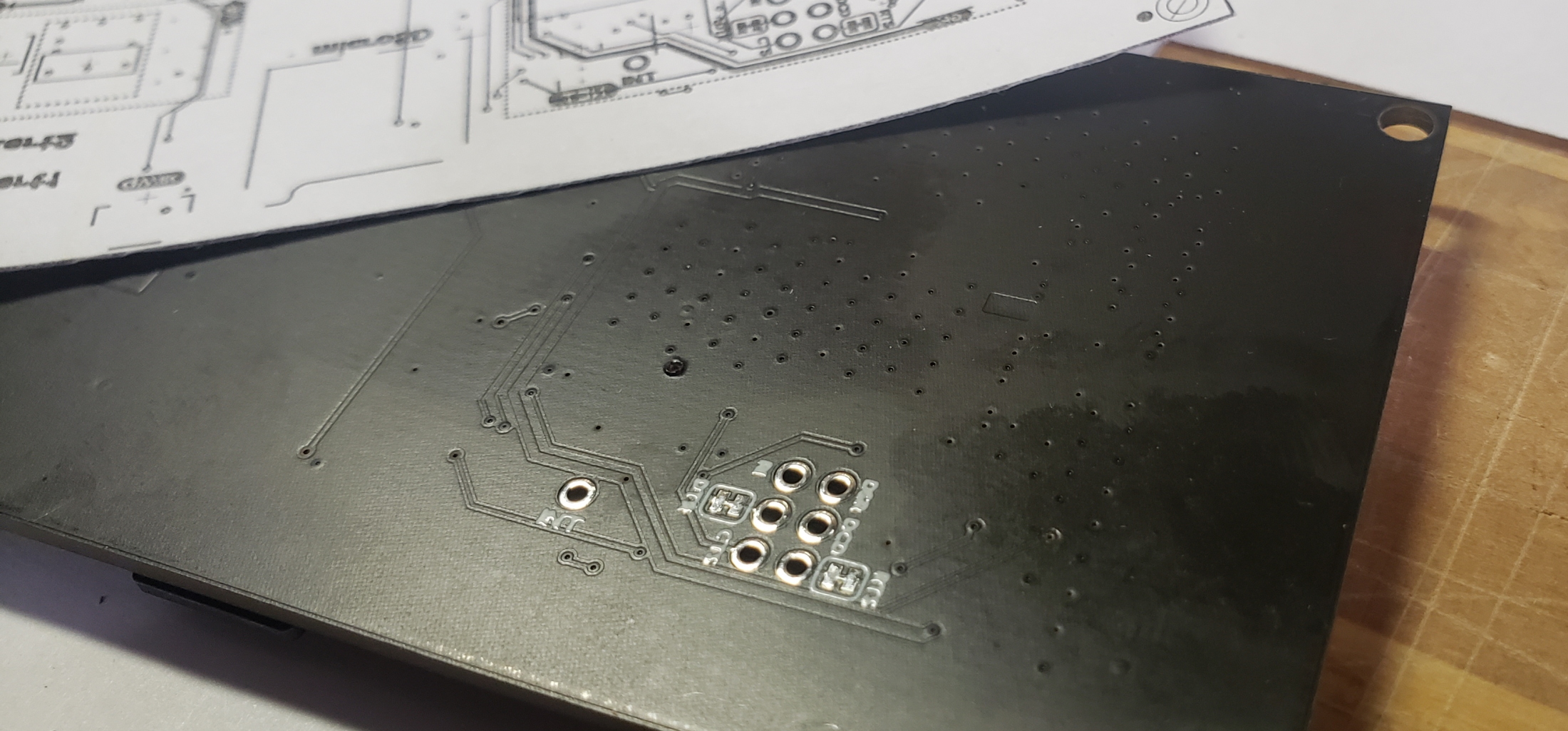
The indentation made all the difference to get the drill in the correct position.
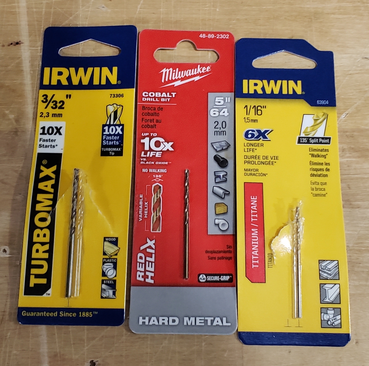
Standard drills from the local hardware store
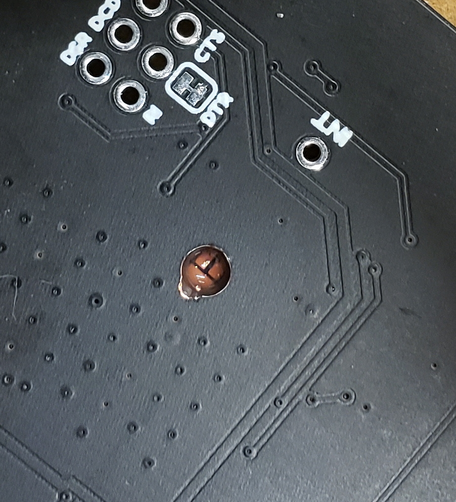
I used two off-the-shelf, standard drill sizes: 1/16” and 3/32”. I used a drill press in the BTU lab at CU to do the initial plunge drilling.
Initial drill with 1/16"
I got through the bottom layers of soldermask, copper and FR4. This is a two-layer board so I stopped drilling when I thought I was close to hitting the top copper layer.
I finished drilling by hand. A sharp bit is surprisingly effective at removing FR4. The drill bit started to get "catchy" once I reached the top copper layer, so I stopped.
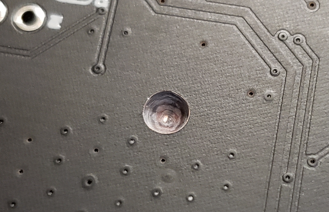
Not much to see..
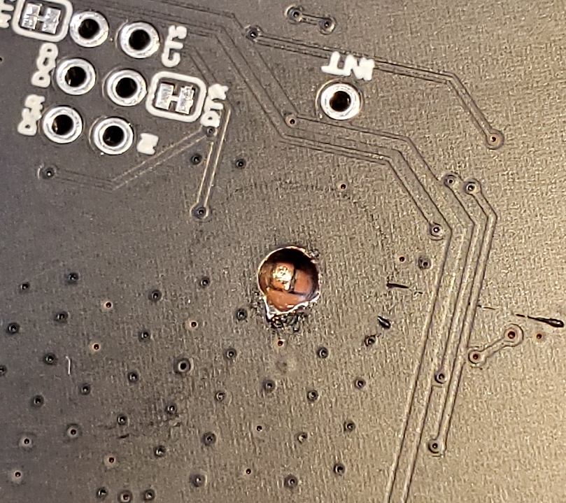
I then switched to the 3/32-inch drill to enlarge the hole. With the larger hole, I was able to insert a multimeter probe. I scraped the side of the wall and tested for continuity between the lower edge of the hole (where I hoped to make contact with the top copper ground plane) and a ground pad near by. Satisfied that I had made it to the top copper layer (at least to the large ground plane), I continued to drill slightly at an angle again with the smaller 1/16-inch drill. At some point I decided to use some isopropyl alcohol with a Q-tip to clean out the fiberglass from the hole…
There be pads!
I was treated to a great surprise! I can see pads! While it was clear where the ground plane was, I couldn't be sure which pad was the power control pad I needed.
The power pad is on the left
A quick check against my map and it was clear that my pad was the one on the left.
Alcohol makes the FR4 transparent
While the alcohol made the fiber glass transparent for a moment, it would quickly evaporate, leaving behind the opaque FR4. It was obvious there was more fiberglass above the pad.
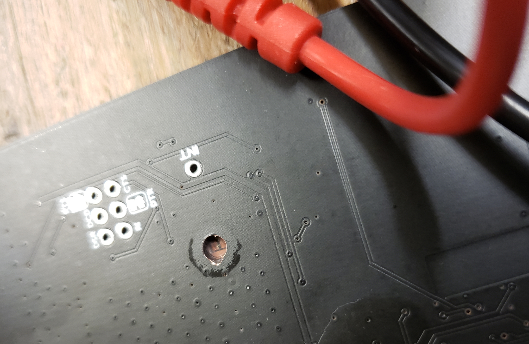
After some more hand drilling I started to see shiny. The hole was big enough to allow for my soldering iron tip but it was a bit awkward. Adding a little flux did two things, including one I didn't expect: flux is great for getting solder to flow where it should, but it also contains a mild acid to clean oxidized contacts. This acid was just what I needed to remove enough FR4 to create a solderable point on the pad.
Not pretty...
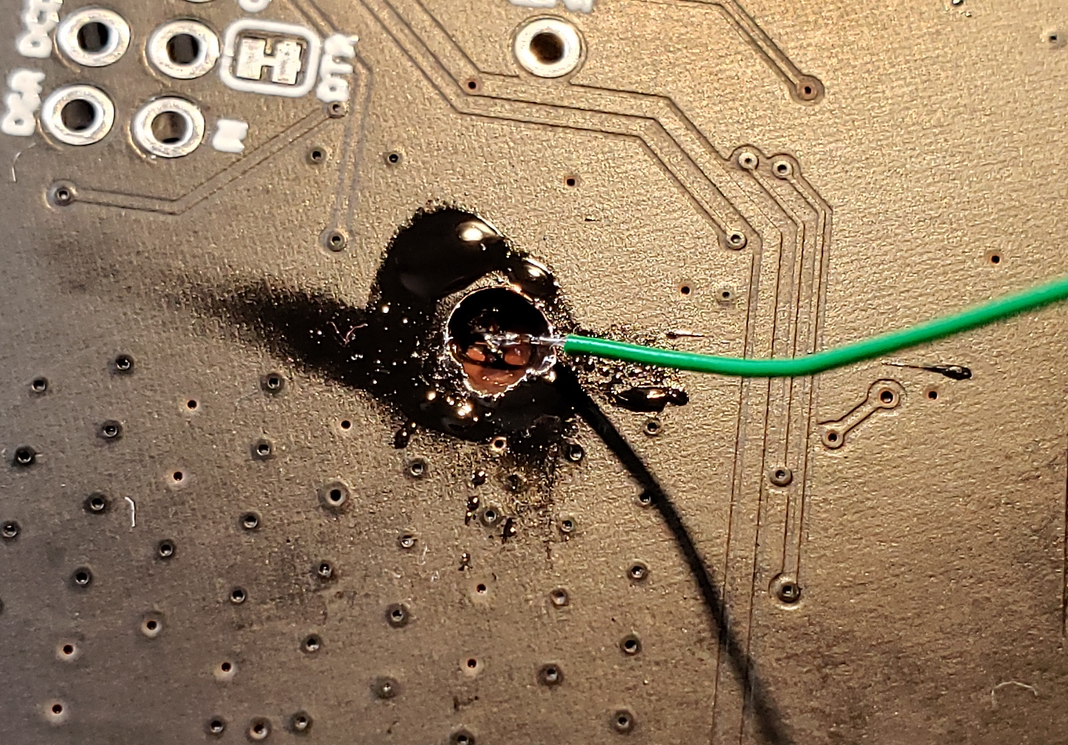
After a few attempts at soldering I eventually transferred enough heat down the exposed 30AWG wire to melt the solder at the tip of the wire down onto the exposed pad. It’s a hack job but the solder connection held with a very light tug. I made a few more continuity checks with a DMM to make sure I hadn't accidentally shorted to the ground plane.
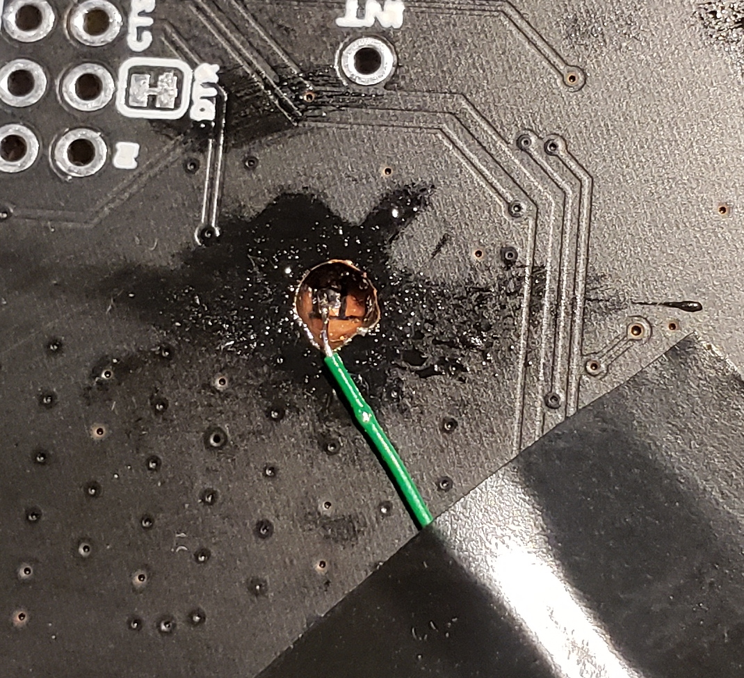
Wire successfully soldered through PCB
The area around the top of the hole is all ground plane. The wire is exposed, so I made sure not to allow the bend to come in contact with the ground plane. Some electrical tape held the wire in place while I soldered the other end of the wire to the microcontroller (the Artemis). A quick test later and some dainty handling of the PCB proved that the cellular module was being turned on! It worked!

I was obviously worried about breaking the solder connection and/or ripping the pad. Once everything electrically tested out I filled the hole and surrounding wire with hot glue. This provided ample protection and strain relief to the wire and solder connection.
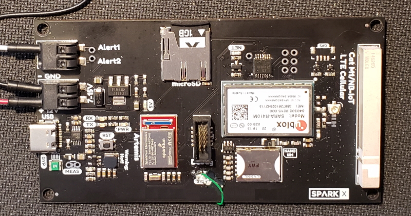
The final working hack job
Obviously this method only worked because I got lucky on a few fronts: the module had large pads that made soldering “easier,” and there were no imperative traces directly below the pads so I could drill from the back. After finding and fixing the power pin issue I continued development and found other problems with my design. Had I immediately stopped after discovering the power pin issue and ran another version of this PCB, I wouldn’t have found the four other problems with the board.
The next time you have a flawed PCB, think twice about how you might be able to make it work.


Loved this. https://hackaday.com/2019/12/27/drill-thrice-solder-once/
Hey Thanks! Great to see it on Hack-A-Day.
If you have to do this again, you might try using an end mill for the hole clean-out. With its flat bottom (as opposed to the pointy end of a drill bit), you can expose more copper in a flat-bottomed hole.
We can learn a lot from our failures! I once had to do something like this to access the traces on the internal layers of a 6 layer PCB. It was very tedious. That taught me to think twice about putting traces on internal layers if I wasn't 100% certain that part of the design would work.
This was educational as well as entertaining. As engineers, I think we are reluctant to talk about 'how the sausage gets made'. Thanks for the article.
You're very welcome!
Excellent article! Never thought about using sticky tack to hold down wires.
Sticky tack is without a doubt my #1 tool recommendation. It's way better than a third hand.
Failures are merely opportunities for ingenuity. By design... ;) I enjoyed this thoroughly!