The Essential Guide to Prototyping your Electronic Hardware Product
Check out the second part in our guest blog series from John Teel of Predictable Designs.

For the next few weeks, John Teel, Founder of Predictable Designs, will be sharing a series of guest blog posts with us, helping readers gain insights into strategy, design thinking, and how to get great product ideas to market. John is an electronics design engineer, serial entrepreneur and blogger, who now focuses on helping hardware entrepreneurs, startups and small companies through his Hardware Academy program. Check out his website for more insights and to learn more.
A new consumer product will go through many prototype iterations before being ready for mass manufacturing. In this article I will teach you exactly what you should be learning with each and every prototype version. Each stage of bringing your electronic product to market will have different prototype requirements. Unfortunately, no single prototype is sufficient for bringing a commercial product all the way to market. No matter how advanced computer-aided design has become, your new product will need multiple prototype iterations before being ready for mass manufacturing.
Prototyping your product is all about learning. Each time you create a prototype version you will, or at least should, learn something new. Always start with the simplest, cheapest way to prototype your product. Then, with each prototype iteration you should progress closer and closer to a production-quality prototype. During the early stages of prototyping it will be best to separate your product into different types of prototypes, each with its own goal.
Proof-of-Concept (POC) Prototype
A proof-of-concept (POC) prototype is, as its name implies, an early stage prototype for proving the basic concept of the product. A POC prototype rarely functions exactly like the final product, and it will never look like the final product. It has only one goal - to prove the fundamental concept of the product at the lowest cost possible.
For the majority of electronic hardware products, a POC prototype will be built on an electronics development kit such as an Arduino or Raspberry Pi. Most electronic products require either a microcontroller or a microprocessor. The Arduino series of development kits are based on microcontrollers, and the Raspberry Pi and BeagleBone are based on microprocessors. A proof-of-concept prototype is usually only used to determine the practicality of a new product idea; it will rarely be seen by customers. Creating one makes the most sense if you have fundamental questions about whether your product can actually solve the intended problem.
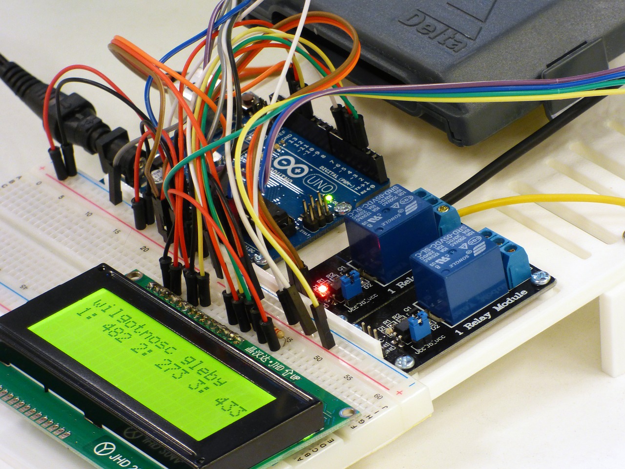
Figure 1: A POC prototype is built from off-the-shelf components and is commonly based on an Arduino or Raspberry Pi.
If there are multiple ways to solve a target problem, but you are unsure of which solution is best, then this prototype can provide a lot of valuable insight. Fundamental questions, such as the basic solution option, are much better determined by a POC prototype than with a custom PCB. If you are technically minded, you may be able to create your own prototype using an Arduino or Raspberry Pi. If you don’t have the skills to create your own POC prototype, and/or you have no major questions about the feasibility of your solution, it is probably better to skip the POC prototype altogether.
Most large tech companies bypass the POC stage, primarily because it’s a quicker path to market to start with a production version. Large companies also have a lot more money, so they can take expensive shortcuts that your average startup cannot afford.
Some design engineers also scoff at the concept of a POC prototype because they know they are rarely similar to the final production version. However, if you have fundamental questions or concerns about your solution, and you have a limited budget, then creating a POC prototype is time well spent. The downside is it increases the time it takes to get your product to market.
Looks-Like Prototype
A common strategy is to separate the appearance and feel of your product from the functionality. These are called looks-like prototypes and works-like prototypes.
A looks-like prototype focuses on optimizing the look, feel, form and aesthetics of the product. For this prototype you’ll use prototyping techniques such as foam, clay, 3D printing, CNC machining, and eventually injection molding.
When prototyping a new product you should separate the appearance of the product from the function of the product.
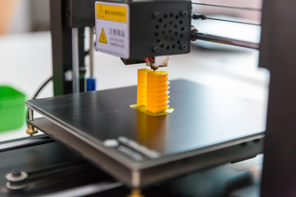
Figure 2: 3D printing is the most common method of producing looks-like prototypes, but CNC machining and even simple options like clay and foam should be not be neglected.
While they may seem overly simple, don’t neglect old techniques like foam and clay, which can be very helpful in the beginning stages. Both of these “technologies” allow you to quickly and cheaply transform a concept into something you can hold in your hand. Using foam or clay can be the cheapest and easiest way to experiment with the size, shape and feel of your product.
With my own electronics product, my earliest prototypes where made of clay. These clay models gave me critical feedback about how the product actually feels in a user’s hands. Starting with clay prototypes may also reduce the number of prototype iterations that you will need when you upgrade to 3D printing. Always start out with the simplest, cheapest methods of prototyping. Learn as much as you can from low cost prototypes before you migrate to more advanced prototyping technologies.
As you work your way up the prototyping technology hierarchy you will find that design changes become more and more complicated to implement. Clay prototypes are trivial to change, 3D printed prototypes are moderately complex/expensive to modify, and injection molded prototypes are the most complex to upgrade. So above all, keep things simple and learn as much as possible before upgrading prototypes.
3D Printing: 3D printing is an additive prototyping process that adds material to create the desired shape. The term 3D printing is a broadly used term that actually refers to various prototyping technologies. Let’s look at the three types of 3D printers in more depth:
Fused Deposition Modeling (FDM): This is the most affordable method of 3D printing and is therefore the most common technology used for home 3D printers. This technology can produce prototypes with a moderate amount of detail. FDM printers work by feeding plastic through a heated nozzle. The material is melted and deposited layer by layer, with each layer fusing to the layer below it. FDM printers are limited in the fine details they can produce so an SLA printer is a better option for complex prototypes.
Stereolithography (SLA): SLA is a more costly process used mainly on high-end home 3D printers and by professional prototype shops. This type of 3D printer works by curing resin with light. The light hardens the liquid resin layer by layer in a process called photopolymerization. SLA is a very accurate method of 3D printing that can make parts with many fine details. SLA printers also produce a much stronger prototype because the layers are chemically bonded together. Prototypes produced by an SLA printer tend to look more professional than ones created with FDM printers. A good strategy for many entrepreneurs is to purchase a low-cost, FDM based 3D printer for producing early prototypes. Once the appearance and strength of the 3D printed prototype become more important you can move to using a professional prototype shop with SLA printers. This strategy will save you money and speed up development for many products.
Selective Laser Sintering (SLS): An SLS system uses a laser to sinter (i.e. harden) powder materials layer by layer to form the desired shape. A big advantage of SLS is it can be used to create metal prototypes. Keep in mind that SLS is too complex for home 3D printers, so it’s only an option when using a professional prototype company.
CNC (Computer Numerical Control) Machining: The opposite of an additive process is a subtractive process. As the name implies a subtractive process removes material to form the desired shape. The process starts with a solid block of plastic or metal. Material is then carved away to form the final sculpted prototype. One of the primary advantages of CNC machining compared to 3D printing is that you have much more flexibility in regards to the material used. Not only can you create prototypes from plastic or metal, but you can select very specific plastic resins which precisely match the material you will use for mass production.
Works-Like Prototype
A works-like prototype is focused on the functionality of your product, which for most electronic products means the internal electronics. A POC prototype can be considered an early version of a works-like prototype, but now it is time to jump from a POC prototype to a production-level, works-like prototype. This means abandoning the use of development kits like Arduino. You now need to develop a custom Printed Circuit Board (PCB) to hold and connect all of your product’s discrete electronic components.
Figure 3: There is a drastic jump in the technical skill to develop a custom PCB compared to the skill needed to make a POC using off-the-shelf components.
Developing a custom PCB for your works-like prototype requires significant engineering design experience. If you are fortunate enough to have these skills (SparkFun side note: or you want to leverage ALC!) then you will save thousands of dollars on development fees. Engineers are expensive and the development of this custom PCB is commonly the most expensive development cost you will face.
Prototyping the electronics:
How you begin prototyping your product’s electronics depends on what questions you are trying to answer. Every time you create a new prototype you should have well-defined questions that the prototype should answer. If you have broad questions about whether your product will even work, or whether it will solve the intended problem, then you should have already started with an early works-like prototype based on a development kit such as an Arduino or Raspberry Pi.
If there are no big questions about your product’s functionality then you should probably move right to designing a custom PCB. Most large companies developing products begin with a custom PCB. This is the fastest route to market, although not likely the cheapest. Prototyping a custom PCB consists of two steps: producing the bare PCB, and soldering on all of the components. We’ll discuss each process separately.
Although there are techniques for producing your own PCBs at home, they are limited to simple designs. So you will most likely need to outsource your PCB prototype production. Assuming you don’t make and assemble your own PCB boards, you’ll use the same process to produce your prototype boards, as well as to manufacture your boards in high volume.
The PCB production is summarized in the following steps:
The process begins with a laminate core made from woven glass epoxy. It serves as an insulator between conducting layers and provides physical strength to the board.
Single-sided boards consist of one laminate core with a copper layer on one side. Double-sided boards consist of a laminate core with copper layers on each side. Multiple layer boards consist of a stack-up of alternating copper layers with laminate core layers. Most boards will use two, four, six or perhaps eight conducting layers.
The layout design for each conducting copper layer is laser plotted on film and a light sensitive chemical “resist” is applied. The copper layers are then exposed to high intensity ultraviolet light which shines through the film. This light hardens the resist layer over any copper traces and pads.
The copper layers are then processed through a chemical solution which removes any of the resist layer that wasn’t hardened by the ultraviolet light. This leaves hardened resist material only over the desired copper traces and pads. Another chemical is then used to remove any exposed copper not covered by resist. The hardened resist layer is then removed, leaving only the desired copper to form the traces and pads.
A lamination process is next used to bond all of the layers together to form the stacked PCB.
Holes are drilled through the PCB stack-up to form vias which are used to connect signals on different layers. Any holes for through-hole components are also drilled. However, it’s generally best to only use surface-mount technology (SMT) components to minimize your soldering costs.
Copper is next deposited on all exposed metal surfaces including the inner walls of any holes. Additional copper is electroplated onto all exposed copper surfaces.
Now that the bare PCB is complete, the next step is to place and solder all of the electronic components. Robotic equipment called a pick-and-place machine uses a vacuum system to pick up the components and precisely place them on the PCB. Solder paste (a sticky mixture of solder and flux) is used to temporarily hold the parts in place.
Finally, the boards are run through a reflow oven to melt the solder paste and form a permanent electrical connection between the component and the PCB pads.
Engineering Prototype
An engineering prototype (also sometimes called a works-like-looks-like prototype) is the first time that appearance and functionality come together in a single prototype. Once you have an engineering prototype you finally have something of sufficient quality to show customers and investors.
Figure 4 - An engineering prototype merges the works-like and looks-like designs together into a single prototype.
This is when it becomes a bit more practical to seek outside investors. By this stage, you’ve moved past most of the engineering and manufacturing risk. Investors obviously love this reduction in risk.
For my own hardware product I funded the product development myself up to this stage. I used my prototype to get a large, national retailer interested in my product. From there, I leveraged that success to find a manufacturer willing to fund the remaining prototype stages.
An engineering prototype is close to the production prototype, but it still hasn’t been tested or prepared for mass production.
Pre-Production Prototype
This is a works-like-looks-like prototype that has been optimized for manufacturing. This is very close to the final product your customers will see. In most cases, it should also include the retail package if the product will be sold via retail outlets.
Although the pre-production prototype may look and function very similar to the works-like-looks-like prototype, the key difference is manufacturability. During product development many entrepreneurs underestimate the work needed to migrate from a prototype to a product that can be efficiently manufactured. Making a few prototypes is completely different than manufacturing millions of units. In most cases, considerable additional design effort is required to prepare the design for mass manufacturing.
For example, 3D printing or CNC machining are typically used when prototyping the product’s enclosure. For mass manufacturing, high-pressure injection molding will be the technology used to produce the enclosure.
3D printing and CNC machining are very forgiving technologies and you can prototype just about any shape of plastic you can imagine. This is not the case with injection molding. Injection molding has very strict production requirements. After you finalize your 3D printed prototypes it will be necessary to further upgrade the design for injection molding.
- Injection Molding: 3D printing is fantastic at producing tens of parts. However, it’s not practical for producing hundreds or thousands of parts. Ultimately, injection molding will be necessary to manufacture your product’s enclosure in higher quantities. Not surprisingly, the injection molding process starts with the creation of a mold. Molds are machined from metal, and the hardness of the metal determines the mold’s lifetime and cost.
For prototyping, or early production, aluminum molds are generally the best choice. Aluminum molds typically cost a couple thousand dollars each and can produce up to about 10,000 parts. The mold forms two halves that are held together as hot, molten plastic is injected at high-pressure into the mold. The high-pressure is necessary in order to produce fine details in the part. Once the plastic cools and solidifies, the mold is opened and the part is removed.
Most designs will require significant modifications in order to prepare them for injection molding. Be sure whoever designs your enclosure understands injection molding, otherwise you are likely to end up with a product that can be prototyped but not manufactured in high volume. Reaching the point of having a fully functional, works-like, looks-like prototype is a huge accomplishment, so pat yourself on the back once you achieve this milestone!
But don’t get too excited just yet... the transition from prototype to mass manufacturing is one of the most underestimated steps to bringing a new hardware product to market.
Engineering Validation Test (EVT)
Once you have a finished engineering prototype it’s time to begin testing it to validate that it works exactly as specified.
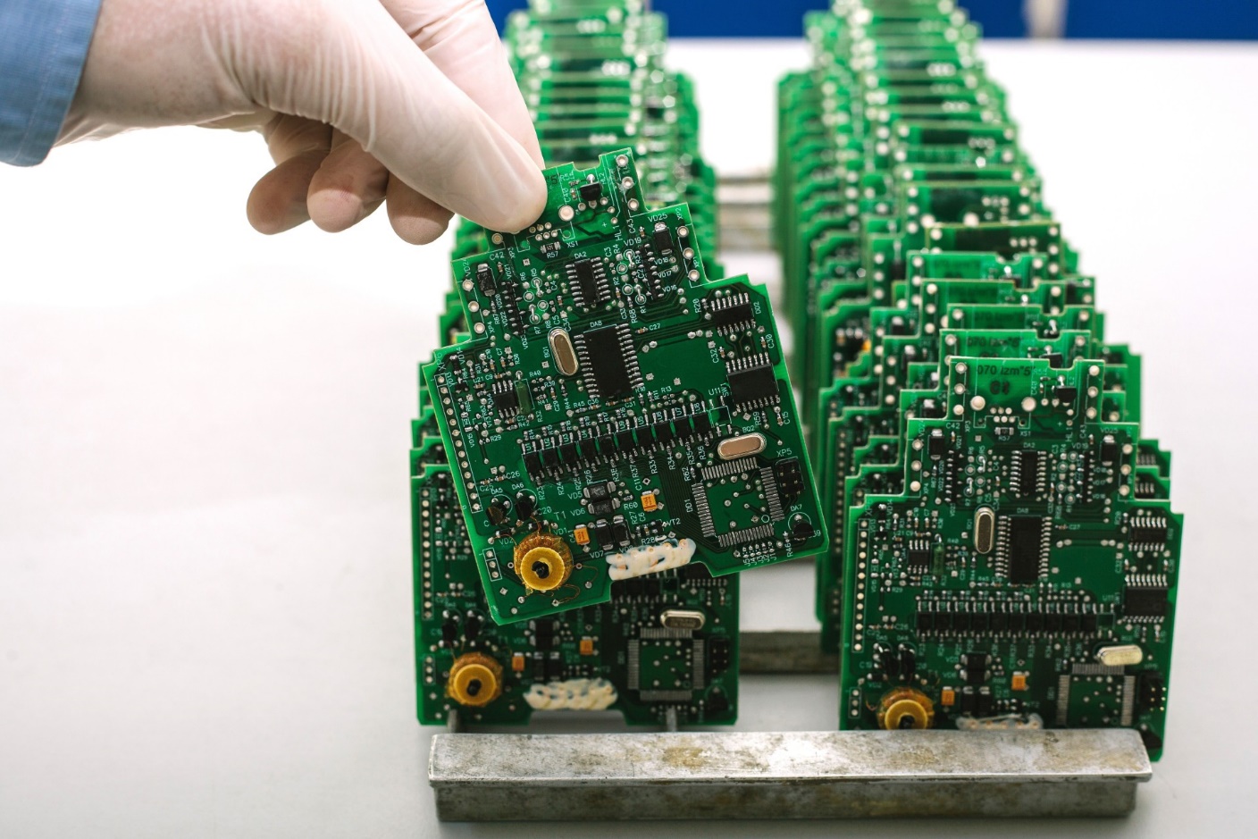
Figure 5 - The goal of the EVT stage is to prove that your product design meets the functional, performance, and reliability requirements.
The first stage of this testing is called Engineering Validation Testing (EVT). This stage of testing focuses on the electronics. Typically between 10-50 units will be tested during EVT. EVT will include testing the basic functionality but also doing various stress tests to ensure there are no hidden problems. This includes power, thermal and EMI testing. The goal of EVT is to validate that your prototype meets the functional, performance, and reliability specifications.
Design Validation Test (DVT)
The Design Validation Test (DVT) is one of the most complex stages. Its goal is to ensure the product meets any necessary cosmetic and environmental specifications. A significantly larger number of units will be needed than for the EVT stage, typically 50-200 units. These units will be very aggressively tested including drop, fire and waterproof testing. Validating that the product is durable enough to withstand day-to-day use is one of the primary goals of design validation testing. This is also commonly the stage at which electrical certifications are obtained. This includes certifications such as FCC, CE, UL and RoHS to name a few. Because of the cost and time required to obtain the necessary electrical certifications, the process is usually delayed until the DVT stage. This is to ensure that no other design changes are required after certification testing begins. Of course, if any problems are found during the certification testing process, then design modifications may be necessary to correct them.
Production Validation and Testing (PVT)
The PVT stage will be your first official production run. You will establish a pilot production line with the priority of optimizing your production process. The focus here will be on improving your scrap rate, assembly time, and quality control process by optimizing your production line, but not by making any further product design changes (unless a serious design issue is discovered). A small pilot production run of several hundred units is typical, and if no problems are found these can be your first units that can be sold!
Conclusion
One of the main things I hope you have learned from this article is that prototyping is a long process requiring many iterations. The prototype journey is complex and not to be underestimated. Don’t be in a rush to move up to more advanced prototyping technologies until you have gained all of the information you can from less complex, lower cost technologies. The idea that you simply create a single prototype (or two) and then just jump into full production should now be clearly seen as a myth.
This article was originally published at PredictableDesigns.com.


Great article, though I have a couple of comments:
On the Proof-of-Concept prototype, in my experience, getting it done quickly is often (far) more important than minimizing cost. I've had times when I needed something (in one case, a couple of sensors) for the PoC, and ordered sensors that had much better specs than what would be needed in the final project simply because they were "in stock", and then paid more than the cost of the sensors to get "two day delivery". (I was able to work on other portions using "parts-on-hand" while waiting for the delivery, so didn't go for "next day delivery".)
One more stage I use before starting the PCB layout, is what I call the "Cardboard Prototype": I take a piece of cardboard the size and shape of what's expected to be the final PCB, and attach actual samples of the major parts that will be used, especially things like connectors, switches, and displays, but also any ICs, large capacitors, etc. (I don't bother with things like small SMD resistors or caps - although I do try to allow some room for them.) Double-stick tape can be helpful, though sometimes a hot-melt glue gun is useful, and any PTH parts can simply have leads pushed through the cardboard and bent to hold the part in place. This can be used to make sure that the end user can easily access critical components, and that everything will fit the proposed case (or help with the case's layout), and also can show up certain "manufacturability" and other issues while assisting in minimizing the size of the PCB.