Enginursday: Innovative Testbed Design (Part 2 of 2)
Join us for part two of our in-depth look at testbed design at SparkFun. Here, we focus on the hardware design choices for our in-house testing tool, the Flying Jalapeno.

This is part two of our series about the history of quality control and testbed design at SparkFun (click here to read part one). There was actually much discussion in the comments about hardware design - thank you so much to all that chimed in! You had very valuable feedback, and I look forward to hearing more after we dive a little deeper into the hardware on this design.
You are welcome to download the Eagle design files from the project GitHub repository here:
For more info on getting started with Eagle, please check out this tutorial: How to Install and Setup Eagle.
For anyone that might prefer to follow along with a PDF, you may also click on the following image:
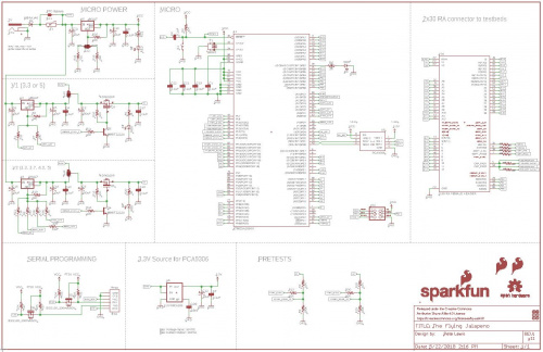
Flying Jalapeno Schematic (PDF LINK)
Power control switching
One of the earliest advancements in testbed design was the ability to control when power is applied to the product. Before this feature, we usually left the pogopin to the product’s VCC “HOT” - meaning that it was permanently wired to a power source. This should work fine, in theory, for most of the time, but what we found was that if you didn’t place the product down perfectly, sometimes you would momentarily short VCC to GND. Note, this would only happen on products where the two header pins VCC and GND were located next to each other, but that was actually pretty common. So during this burst of current on VCC, our testbed power supplied didn’t really like this, and they would drop voltage causing the entire testbed to reset. Ugh!
Some of the first testbeds to incorporate power control actually just routed an IO pin directly from the testbed ATMega328 to the VCC on the product. In this case, we could supply power to the product, but were limited to the 40mA (or so) that the IO could provide. Definitely not the best solution, and we saw a few testbeds die, and so the progress continued.

|

|
| Power switch schematic close up | Power Switch highlight on board |
The next approach was to try a high-side switch using a mosfet. Looking back, we could have just as easily done it with a relay, but didn’t have an ideal relay in our inventory. Now that we have some nice mini relays like the SparkX Qwiic Relay, that may be the preferred way. But at the time (2009-ish), we only had the Beefcake Relay Control Kit, which seemed like overkill for 99 percent of our products. You’ll notice we also added a transistor on the front end to ensure the mosfet opens fully and takes the load off of the IO pin on the micro, and it’s really quite nice that writing the control pin HIGH actually engages power. We are always trying to think about usability, even with in-house tools.
Testing for shorts to ground
Using a simple voltage divider style circuit, a digital control pin and an analog read pin, we can safely and easily test a product's power line (aka VCC) for a short to GND. It is particularly nice to know this before powering up a product - especially when it is a high-current product. We actually test for shorts to GND on all products now, regardless of power consumption. Odds are the testbed and product would survive a few hundred surges, but after a few too many, you are on the quick path to destruction. When designing for production, we need to think about testbeds living on (and working well) for many years to come.
I should also note that we commonly refer to this test for shorts to GND as the “pre-test.” This is because the “main” test is usually referred to as just the “test.”
The pre-test circuit is actually a pretty good exercise in learning about voltage dividers. If you’d like to learn more check out this tutorial here.

|

|
| Pre-test for shorts to ground schematic close up | Pre-test highlight on board |
We use the circuit shown above to see whether or not there is a GND connection (or something that pulls as much current as GND would) on the product’s VCC. When there is a short, then the two 10K resistors basically split the VCC and the ADC reads the magic dreaded “486.” When there is no short, it will essentially form another voltage divider between a 100K and a 10K, and the ADC reading will be much higher. For a more info on this circuit, please check out a previous blog about quality control here.
Capacitive Touch "Buttons"
We moved away from mechanical momentary switches to engage testing years ago. A capsense pad (most importantly, non-mechanical) is much more reliable over thousands and thousands of “presses.”

|

|
| Capacitive Sense schematic close up | Capacitive Sense Resistors highlight on board |
We use the Arduino capacitive touch library and two IO pins with a large resistor. Because we often need two buttons on a test fixture, we opted to dedicate four IO pins and include the resistors into the Flying Jalapeno design. With this setup, we simply need to route a trace to a pad on the daughter testbed. Note: we do usually take extra care on these traces and route them with 0.02 inch (20 mils) width. By avoiding vias and other data lines, we have seen great results with this form of capsense. Mad-house-routed thin traces or bad ground pour flow can make for some really wonky readings.
Dedicated LED IO with Built-in Resistors
We pretty much always need four LEDs on the testbeds these days – PASS/FAIL for the pre-test for shorts to GND, and PASS/FAIL for the main test. Because we have plenty of extra IOs on the ATMega2560, we decided to include the current limiting resistors on the FJ. These pins are now fairly committed for LED use, but we’ve got plenty of IOs to spare. This way, the daughter boards simply need a trace to an LED on each of these lines. The less complex the daughter boards can be, the better!
I2C Isolation “Switch”
A lot of early testbeds that involved I2C were troublesome for us. It was pretty common for I2C testbeds to “lock up” during testing. This was usually due to the testbed trying to talk to a product that was broken, had cold solder joints or had jumpers on SDA or SCL. I seem to remember a glorious day when wire.end() actually started working... Until then, we used to (and still do) disconnect the lines with a mux built into the test fixture.

|

|
| I2C "isolation" switch schematic close up | I2C "isolation" switch highlight on board |
Again, at the time, we didn’t really have an ideal switch, and the Beefcake seemed like overkill for data lines, so we opted to use the PCA3906 I2C converter IC we had on hand. It had an enable pin that proved to be useful in disconnecting. We found that if we disconnected the I2C lines with something like this (in between testing boards), then it was much less likely to lock up. And best of all, the techs were much less likely to wear out the old fashioned momentary reset button the test fixture.
ATMega2560

|

|
| ATMega2560 schematic close up | ATMega2560 highlight on board |
We simply went with this because it was very similar to our RedBoard, but with many more IOs. Sometimes a testbed will require a few more IO than the ATMega328 has to offer, so we found ourselves either using a mux or shift registers – better safe than sorry when it comes to having enough IOs. Also, having an Arduino-compatible testbed brain meant that we could more often than not utilize some of the product example codes for the test fixture.
The test developer also serves as a good beta tester for the products they work on. Usually the engineer on the product design has some sort of working code ready before we launch (which is super handy for test development). But sometimes even more importantly, getting it to work on the test fixture can help discover some bugs or documentation confusion before we officially go live with it on SparkFun.com.
Logic Level Select Jumper
Taking a tip from our breadboard power supply, we opted to add in a logic level select jumper.

|

|
| Logic Level Select schematic close up | Logic Level Select highlight on board |
There was some discussion as to whether we wanted a slide switch or jumper. We ultimately wanted to keep it a jumper, so that it couldn’t be accidentally switched during handling and cause issues for testing. Plus, there is always gonna be some soldering assembly work for the daughter boards, so what’s the trouble in setting a quick jumper as well? Also, you may note that we are doing a “no-no” here by running the ATMega2560 at 3.3V - it is slightly out of spec for a 16MHz crystal, but we have seen minimal issues (if any at all) caused by this, so we’re gonna keep running with it.
Software-Definable VReg Control on Two Power Sources
Taking the selectable VReg idea one step further, we decided to make the two power sources have adjustable outputs that were software defined. By connecting various resistors to IO on the micro, we can choose which resistor we’d like to “send to GND” by writing that corresponding IO LOW. This effectively sets the output of our VRegs.

|

|
| Software Definable Voltage schematic close up | Software Definable Voltage highlight on board |
You'll notice that V1 can do 3.3V or 5V, and V2 can do 3.3, 3.7, 4.2 or 5V. This is nice when emulating a charged or empty single cell LiPo battery. By bouncing V2 between 3.7 and 4.2, we can get charge circuits to engage or disengage. This has proven very handy when it comes to getting a charge LED to blink.
2x30 RA Header
There was much discussion about what type of connector would do the job. It was tough to find the balance between strength, current capabilities, size and design-ability. We opted to go with a PCB-to-PCB right-angled style connector, and the 2mm pitched RA 2x30 header we found had a 2A rating, so it fit the bill. We also opted to have some connections with redundant pins (GND, V1, V2). Not only was this a good thing for reliability, it gave us way more current capability than we’d ever need (famous last words). More connection means less resistance too, so I was glad to know we’d see very minimal voltage drop from source to pogopin.
Mounting Brackets
With our choice of connector, this required a little creativity on how to mechanically connect the FJ to the daughter boards. We did not want to rely solely on the headers themselves, and so came up with some mounting brackets on either side.
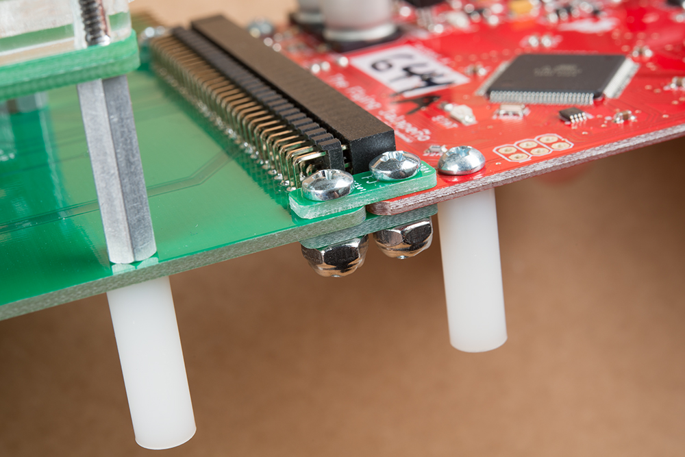
They go on either side of the connector, on the top and the bottom, and are held into place with a 4-40 screw with a nylon thread locking nut. The spacing of the drill bits also ensures that the FJ and the daughter board will be assembled at the exact spacing for every future testbed. This is nice, because we want to make sure that the 2x30 is inserted fully. Yet another benefit that I didn’t anticipate (and was pleasantly surprised while building up the first prototype), is that these brackets worked as a nice “jig” to hold them together while soldering in the 2x30 male connector on the daughter board.
Custom Eagle Part

|

|
| Eagle Symbol | Eagle Package |
To make daughter board design faster, we opted to create a custom part in Eagle. This way, we could quickly drop in an FJ into any daughter board design, and have all of the connections easily accessible. Note: we created the female and male versions of the connector in the same device. This makes it easier when referencing the FJ design during any troubleshooting. Also, we opted to include quite a bit of “used pins” in the symbol, which help highlight what they are doing upstream and can help with developing code for this hardware. Although, using the code library in conjunction with this hardware makes life even easier.
Logic Level Conversion for Serial Debug

|

|
| Serial Logic Level Conversion schematic close up | Serial Logic Level Conversion highlight on board |
Do you suffer from serial bridge logic level conversion problems? We do too. Around production and at most engineers' desks here at SparkFun, it is always impossible to find the right logic level version of the serial bridge. Also, it is probably one of the most common mistakes made around here - “whoops, I plugged in a 3.3V logic thing into a 5V thing,” or vice versa. Well, with the FJ, we had a chance to avoid this problem, so we did. A tech can plug in any variety of serial bridge tools into the FJ, and it has the logic level conversion to handle it. Whew!
A Future Hardware Revision
As with all projects, this will never truly be done. The Flying Jalapeno has some quirks that could be improved (thank you for all your feedback on our previous post). But after two rounds of prototypes, we are fortunate that nothing supercritical is a road blocker right now, and for the most part the Flying Jalapeno is doing its job quite well. Nevertheless, here are some of the things we are considering on the next revision:
Upgrade mux switch for I2C isolation. The original IC choice for the I2C isolation was not really the best IC for the job. When we need to switch a connection on most newer testbed designs, we opt to use the 74LVC4066 MUX 1:1 (x4). This has worked great for switching all of our RX/TX, USB D+/D-, and programming lines. We also used this on a recent programming tool for production: the Pi AVR Programmer HAT (https://www.sparkfun.com/products/14747), and it has been holding up well for all our 2MHz + programming speeds.
Additional GND connections on the right side of the header package. Sometimes it can be a challenge to get a good ground flow all the way around the daughter board, so if I were to do this again, I’d sacrifice a couple IOs to be GND connection points on the right side of the connecter.
Additional dedicated LED IO with resistors built in. We are finding that with most daughter boards, we usually need one or two more LEDs. In addition to the standard pass or fail LEDs, it’s nice to indicate the tech other statuses or instruct them that it is time to do a certain action. You can’t have too many LEDs!
A strange issue with power control. Maybe someone reading can help us with this, but strangely enough, the power control circuits seem to be interacting. When V1 is powered up, and V2 is powered down, there still is some voltage present on V2. We even tried removing the source of power on V2, and it shows the same condition. I’m guessing it has something to do with the two long traces perfectly parallel to each other. Most of the time, this is not a problem (because we have them both powered up during testing), so we've been able to get by with the current version of the hardware. But it sure would be great to get to the root of what's causing this, so any thoughts would be very welcome. Thanks!
Note, if you like to jump to part 1 of this blog, click here:


I've got lots to say, but no time to type today (medical appts, etc.). Hopefully tonight or tomorrow... just a "heads up" for those interested to check back in a couple of days. ;-)
Hey 773, I was hoping you'd chime in here. Thanks! Hope your appointments go well, and we look forward to reading your feedback! I'll be watching my inbox :)
Parallel traces do not couple DC levels - neither capacitive nor inductive coupling will explain DC voltage crossing from V1 to V2 when adequate drain resistors (R20/D4 is enough) are present. There is a direct cross conduction path between V1/R3/R13/R30/R28/V2 which may explain some of your issue.
Hey stcarlso, Thanks for taking a closer look at my design! Could you explain more about what a direct cross conduction path is? (or at least help me find some links). All of my searching on google is leading to stuff about the human heart :)
[edit] Ahhh.... whoops. I was reading waaaay to much into your words. Yeah, I see that they are connected via resistors. I think the "cross" was throwing me off. You are definitely right, though. Thanks for finding this and commenting!!
"Note: we do usually take extra care on these traces and route them with 20-millimeter width."
Probably mils?
Hey 966, Thanks for catching that. You are definitely correct. 20 millimeters would be just a tad bit excessive :). Fixed. And thanks!
PS what terminology do you prefer when talking about trace width? I think the norm around here at SparkFun is to say "20 mils" or sometimes "20 thou".
When researching PCB design tips a few years ago I came across the saying "thou shalt always use thou." By trying to get into this habit we can avoid exactly this confusion.
Regardless of whether you come from an imperial or metric background, the "milli-inch" unit is just wierd.
Did I miss the reveal on the design flaws from part 1? Or at least the one you were hinting at that no one figured out?
I agree with stcarlso, you have a signal path from V1 to V2 through R3-R13-R30-R28 in your PRETESTS circuits (and also to the processor GPIO). Both PRETEST circuits use the same GPIO to control them so even though they are really driven from the micro there will still potentially be some leakage that affects/biases the GPIO a little. Alternatively the voltage you are seeing may actually be just from the GPIO back feeding into the supply through the PRETEST resistors ?
Dang, you guys are good! Thanks for chiming in stcarlso and Garfieldboy. I can't believe I failed to look at the pre-test circuits!!! They are so obviously related closely to V1 and V2 :)
I will try removing each of the "CTRL resistors" (R13/R30), and see if the problem persists. Maybe a future design will have separate control line IO for each pre-test. We certainly have plenty of IO to spare on the mega2560.
Thanks again. It sure is amazing how a fresh set of eyes on a problem can clearly see what I've been missing for so long.
I will update with results as soon as I have a chance to test this out.(should be early next week)
Hey dksmall, Oops, sorry I didn't reveal the design flaw yet. Here is it:
The one I was thinking of has to do with the fact that the logic level selection jumpers allows you to select 3.3V and this is out of spec for the 16MHz crystal. An ATMega328p says that for operating above 10MHz, you need at least a logic level of 4.5V.
On page one of the ATMega Datasheet, under "Speed Grades" it states:
– ATmega328P: 0 - 4 MHz @ 1.8 - 5.5V, 0 - 10 MHz @ 2.7 - 5.5V, 0 - 20 MHz @ 4.5 - 5.5V
I know this isn't actually that horrible of design practice to be at 3.3V (and is found on some of our other products (for example: the Blackboard), but I was hoping that ya'll would be able to see that from the high res image - just looking at the silk).
We usually aren't "maxing out" the micro in any way on test jigs, so we haven't seen any problems operating at 3.3V with the 16MHz crystal.
Have you (or anyone else reading) ever had issues when you are operating slightly out of spec? My guess is that trying to operate UART or SPI at higher buads would start showing some failures. Are there any other areas of the micro that would potentially start malfunctioning?
I was really stoked to see all of the other feedback though. There is some really good stuff in there! And we all really appreciate you sharing those pictures of your test jigs. It is so fun to see the progression from way back in the 80s!!
With all the years I worked in the semiconductor industry, I'm well aware that those "grades" are guarantees that the part will work at those speeds at the entire temperature range. When I visited SparkFun (you were my tour guide, Pete), the facility seemed to be reasonably close to "room temperature" (often taken to be 25C). Table 26.1 on p. 313 of the Datasheet says that the operating temperature range is -55C to +125C, so you should be pretty safe. Also note that Figure 26-3 on page 318 suggest that the "safe" operating speed at 3.3V is about 13 MHz, so you're not "overclocking" by that much. When I was working for a company that made processors back in the early 80s, we knew that there were a couple of rarely-used instructions actualy started failing at a certain speed, but if you avoided using those instructions, the parts would actually work to several times the "rated" speed (if I remember correctly, over 20MHz for a 6MHz rated part).
Hey 773, Thanks for chiming in here. It's not very often that I think about temperature range when designing the micro controller section of a board. Usually, I'm only thinking about temperature when working with power layouts, resistors/LEDs, and especially a linear vreg.
I once had a product "work" for many years, and then started seeing returns and realized that my power input linear vreg was heating up too much, and if in the right conditions (hot day in a black enclosure), it wouldn't survive very long. Thanks for the tip, and I will make sure to keep temperature as an important variable to consider in all aspects of design.
Glad to hear that we are most likely gonna be fine with the 3.3V logic and 16MHz crystals. These Flying Jalapeno testbed designs will very rarely (if ever) leave our production floor, so at least we have that going for us :)
Without the schematic there's no way of knowing that the solder jumper controlled VCC going into the micro. The jumper could select VCC for the I/O, while the micro always runs off a fixed supply.
Have you been on AVRFreaks? That's the technical forums for the AVR processors and occasionally you will see the topis about overclocking the AVR's. From what I recall the general consensus is yeah go ahead and do it with a one-off or a proto, but don't do it for production units.
Hey dksmall, Good point about the jumper. It is definitely pretty hard to see what's really going on with a design without a schematic. Sorry I assumed that the "VCC" would imply the logic level for the micro. This is what I have learned and is probably pretty bad practice. It looks like there is much more to learn about VCC from the discussion on this post about the difference between VCC, VDD, VEE and VSS.
I'll admit, I should have thought through my challenge a bit more before posting it in the end of my part 1. It was sort of a last second thing I thought of while writing the end of my post, and wasn't originally planning on doing a "contest". Looking back on this, I should have posted the schematic as well (maybe even the eagle files). But for what it's worth, I was really amazed by what everyone was able to understand and point out other flaws from only looking at the picture, and I truly appreciate all of the conversation!
Also, thanks for the tip about AVRFreaks. I remember visiting there many years ago, but it seems to have fallen off my radar lately. I will definitely be checking that out some more.
Actually, that is not a hardware flaw. Out of the gate every Atmel micro has the ClockDiv8 fuse programmed. This is explicitly so every user can make their desired clock selection without exceeding the rating, since dividing by 8 assures you have a safe speed. Leaving that fuse programmed makes it a simple software issue, if you are running at 3.3V and want to play it strictly "by the book" all you need do is never select /1 on the clock divisor. /2 will give you 8MHz which is probably fast enough and within bounds at any of the voltages you are using.
If you are using a bootloader like Optiboot you will need to take this into account when you build and flash it. Set it to run at the default /8 speed of 2MHz and you are good to go.
This is my first comment on SparkFun.
First, thank you for sharing the design. It is a very interesting subject, and I wish more people would share how they test their products.
Someone already commented about switching power supply. The board should have one before the linear regulator. My guess is that you power the board with an external one.
Some suggestions.
1) A reverse mounted PMOS before Q3 and Q5 for reverse current protection. 2) You only have high-side switches for U3 and U4. Add low-side ground switches a swell. Let's say you have a product with two power supplies, and lets say the ground wire of one cable is broken. If you can selectively disable a ground connection, you can test for that broken wire. 3) I'd suggest a current sensor after each regulator to test if the product draws excessive power. 4) Use a regulator that can go as low as 0.5V or even lower. For short-to-ground test, you want your reference voltage to be as low as possible. 5) Use NMOS to control the regulators' voltages.
A nice design. For this type of electronics, you can add a bunch of features and still one day find something is missing. So there is only a good-enough design, never a perfect one.
A couple of points based on looking at your schematic:
1) I would not use NPN BJTs to drive your high-side P channel FETs. If you are worried about drawing current from the Atmega2560 I/O pins, you should use N channel FETs in place of the NPN BJTs since N channel FETs do not sink any current at the gate in order to turn on. A good example of an N channel FET you could use for this would be the IRFML8244, at 3.3V on the gate the part is fully on. And you also can get rid of the 100 Ohm resistors if you use N channel FETs.
2) Consider replacing the U3 and U4 LDOs with switching power supplies. You are going to dissipate a lot of heat in the LDOs if you draw more than a few hundred mili-Amps and you are running with a 12 Volt wall-wart. Assuming 0.3 Amps on the 5 Volt supply --> 12-5 x 0.3 = 2.1 Watts. Thats a lot of power for those small parts and if you don't have a large enough heatsink in the copper on the board they will probably get very hot. If you change to a switching power supply like the AOZ1280, you are good for at least an Amp and you will dissipate a lot less power without having to worry about heatsinking. That should give you more flexibility in the power draw for your daughter boards. The main downside with this approach is you will have increased voltage ripple on your power supplies, but with plenty of carefully placed bypass capacitors and series filtering (inductors, ferrites) you can minimize any problems that causes.
3) As for selecting different power supply voltages, there are many ways to do this. If you are going to use the method of selecting different resistors with Atmega2560 I/O pins as you did in this design, I would recommend isolating the I/O pins from the regulator with N channel FETs. At least if you do that, you don't leave the possibility of any current from the regulator getting in through the static diodes of the Atmega2560 and causing problems. Just drive an N FET gate with the I/O pin, put the source to ground, and put the drain to your selection resistor.
Another way you could accomplish variable supply voltages, and one that would give you a lot more control over what voltage you get out, is to use a digital potentiometer. These can be controlled over SPI or I2C and will essentially allow you to set your supply voltage to anything you want. If you put a regular resistor divider for the feedback on the regulator, and then put the digital potentiometer with the wiper terminal on ground and the A or B terminal at the center of the divider you can set the feedback voltage by changing the digital pot value. You just have to be careful that in software you don't go past the bounds of allowed supply voltages. But you could easily control that by writing a software loop to step the potentiometer resistance and then check the reading that you got with your pretest circuit, until you get to the desired voltage. If you're careful about how you write your code you would essentially have a programmable power supply. And if you use a DC-DC converter your output could range anywhere from 0 to 16V (your max listed input voltage) at 1 Amp output current. That would likely be more than enough range for most of your test boards.
4) I would recommend driving your pretest circuits (signal "44/PT_CTRL") with a high side P FET switch or at least an op-amp configured as a buffer to isolate the Atmega2560 I/O pin from V1 and V2. You don't want the microcontroller to sink current (albeit very little) on these lines. I would also use an op-amp buffer on "A14/PT_READ_V1" and "A15/PT_READ_V2" to isolate the microcontroller ADC from these signals. Isolation is never a bad idea except for the fact that it takes more parts. You probably aren't going to make a million of these boards and I would guess that reliability is more important than a few extra dollars per board.
Pete, I trust that you'll realize that nothing is meant as an "attack", but is meant as constructive suggestions, recognizing that many of them are things that are not in the immediate future but are longer term things. I'm putting it out on the blog as I hope that, in the spirit of Open Source, others can benefit, too.
For others (I'm sure you're aware of this, Pete) I'll mention that I've been "doing" electronics for more than half a century, and "doing" computers since a few weeks after Neil Armstrong took his "one small step". (The 50th anniversary of that will be this year!) More than a quarter century of that experience has been in testing at one level or another. I've done everything from being the operator who plugged the UUT (Unit Under Test) into the socket, push the "start" button, and then put the UUT into the "good" or "bad" box (that was when I took a year off from college and worked in an electronics factory) to making a major change to the "architecture" of a critical part of testers used to test hundreds of millions of parts that reduced the cost of most people's computers by a few pennies for more than a decade.
On the subject of power supplies, IM[Not So]HO, having totally separate supplies for the tester's electronics and the UUT is worth while. It prevents a "disaster part" from causing the tester controller from going into the weeds, and noise from the tester getting into the UUT. For this device, a separate "wall wart" supplying the "MICRO POWER" and one for "V1" and "V2" (with a protection diode and fuse on each wall wart) should suffice. I also think that LEDs just downstream from the fuses can help prevent demonstrations of the "zeroth basic law of Electrical Engineering: it usually helps to plug it in!" (We've all had lots of times when we tracked down the problem to "no power"...). By the way, there are power supplies that can tollerate having their outputs shorted to ground. Also, depending on how many test stations you envision using at any one time, it might be worth while to invest in "programmable" supplies (that the computer controls) for driving the UUT, where the power supply can be told what current limit to use (and even what voltage to supply). It should be possible to come up with a way to easily connect one to a board like the Flying Jalapeno, and disconnecting it when done so it's available for the next batch of (different) units to be tested.
I'd be inclined to include a way to measure the current drawn by each UUT. I'm a big fan of doing datalogging, too, and this info can be VERY useful in detecting certain types of failures. (Can you say "backwards parts"?) Datalogs can consist of simply writing some key data such as power supply current measurements and "pass" or "fail" results (and what step "failed") to a file on an SD card as a CSV file, Time stamps are nice, and this is one reason why I'm not a big fan of Atmel processors, as many other suppliers included RTCCs (Real Time Clock Calendars) on-chip, but that's sort of beside the point. Datalogs are one of those things that, like a fire extinguisher, it's a lot easier to have and not need than to need and not have.
Another general comment is that it is not a really good idea to have pins of the test control CPU connect directly to the UUT -- some sort of a buffer chip, preferably in sockets, are a good idea. (I saw this back in my days of being a "bio-robotic parts handler" when a UUT that had two optoisolators had one unit that had both of them installed backwards. I wasn't operating that machine that night [I worked nights], but you could hear the lady who was operating it scream throughout the whole factory when the two optoisolators exploded, taking significant parts of the tester out. That machine was out of commission for several weeks, and the test adapter was completely redesigned to prevent a recurrance of the problem.). You can put this isolation out on the daughter cards,
As a general comment, I'm a big fan of the tester being able to communicate info back to the operator. There are several 16x2 LCDs on the store front that could be used. (For instance, it could cause the "charge LED" on the UUT to blink and ask the operator "Is the charge LED blinking?" and then the operator would touch one of the buttons in response.)
Speaking of buttons, yeah, you need to use ones that have a high cycle life. Switches used in keyboards, e.g., "Cherry" switches, could be a good choice, as would be "arcade" switches. I'll admit that I haven't used capacitive buttons, but since they have zero moving parts, they should be a good choice as well.
I'll also respond to the CPU speed as a reply to the messages there.
'773
P.S. The appointments went well. Thanks!
I agree with all the suggestion, especially the analog buffer one. You can easily damage the analog pins of your testers. It's better to add some quad op-amps configured as voltage followers before the ADC pins.